Atomic Force Microscopy (AFM) is a powerful and versatile nanoscale imaging technique that has revolutionized our understanding of surfaces and materials at the atomic and molecular scale. By enabling high-resolution imaging, force measurement, and manipulation of materials on the nanometer scale, AFM has become an indispensable tool in various fields such as materials science, biology, and nanotechnology.
At the heart of AFM lies the principle of probing surface topography and properties by scanning a sharp tip over a sample while maintaining a constant force or constant height between the tip and the sample. The interaction forces between the tip and the sample are detected and converted into meaningful data, providing insights into surface features, roughness, adhesion, elasticity, and more. One of the key advancements in AFM technology is the development of various sensor methods to measure these interaction forces accurately.
In this article we will discuss the principles, advantages and disadvantages of different methods used to detect the deflection or force applied to the AFM probe tip with special focus on Piezoresponse Force Microscopy (PFM) with interferometric displacement sensing (IDS) using LDV technology.
Optical beam detection - the detection workhorse in Atomic Force Microscopy
Virtually all commercial AFMs today use what is known as “optical beam detection” (OBD), sometimes called just “beam bounce” detection to sense the displacement of the tip. As shown in Figure 1, a beam of light (typically from a laser diode or superluminescent diode source) is focused on the back of the cantilever.
The beam is reflected by the cantilever onto a split quadrant photodetector, centred such that the intensity on each quadrant is roughly equal. As the cantilever bends, the angle of the reflected beam changes the position of the spot on the detector. If the cantilever bends up or down, the spot shifts vertically.
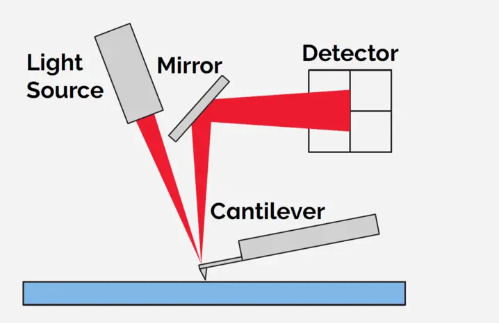
If it twists, the spot on the detector shifts laterally. These shifts are measured by the changing ratios of light intensity on the detector quadrants. This technique was developed soon after AFM itself, and yet it remains the dominant deflection detection technique because it is simple and inexpensive to implement and offers impressively low detection noise (typically 200-300 fm/√Hz).
Although this standard method has proven itself in countless applications, there are problems where the method reaches its limits due to special forces acting on the probe tip. One of these cases is Piezoresponse Force Microscopy (PFM).
Characterizing piezoelectric and ferroelectric materials with PFM measurements
Piezoresponse Force Microscopy (PFM), which is based on AFM technology, has become the most powerful technique for nanoscale characterization of piezoelectric and ferroelectric materials since its development in the early nineties.
The piezoelectric effect refers to materials that generate electrical charge under applied mechanical stress. However, the same materials exhibit the converse piezoelectric effect wherein they mechanically deform in response to an applied electric field. This is the basis of all PFM techniques. In the most basic implementation, a conductive AFM tip is placed in contact with a piezoelectric or ferroelectric sample and an AC electrical bias is applied to the sample through the cantilever (Vtip). The sample deforms due to the electric field and this couples into the deflection of the cantilever. The cantilever detection optics of the AFM measures this deflection, which is then routed to a lock-in amplifier where both the amplitude and phase of the signal are recovered. The amplitude (A) is proportional to the magnitude of the effective piezoelectric coupling coefficient (deff = A/Vtip) while the phase indicates the polarization direction.
The signal-to-noise of PFM measurements can limit applications on materials with very low electromechanical response. To overcome this obstacle, various measures are taken to increase the sensitivity of the measurement method and to avoid artifacts – in depth discussion on these artifacts is beyond the scope of this article. Despite all these tricky efforts another resonance-related artifact remains. This remaining artifact results from a combination of the optical beam detection (OBD) method and electrostatic forces between the cantilever and the sample. Even in the absence of any genuine electromechanical response in the sample, the AC bias applied between the probe and sample can excite the cantilever resonance via an electrostatic (capacitive) force between cantilever and sample.
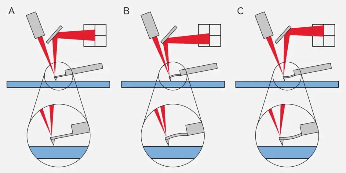
While the probe tip itself is not moving in this case, the cantilever resonance results in a bending of the cantilever according to its characteristic bending modes. These angular changes in the cantilever are detected by the OBD method even though the tip itself is static (Figure 2). In other words, the OBD method is inherently a measure of cantilever angular changes, which can occur even in the absence of vertical tip motion.
LDV helps to overcome OBD artifacts in PFM measurements
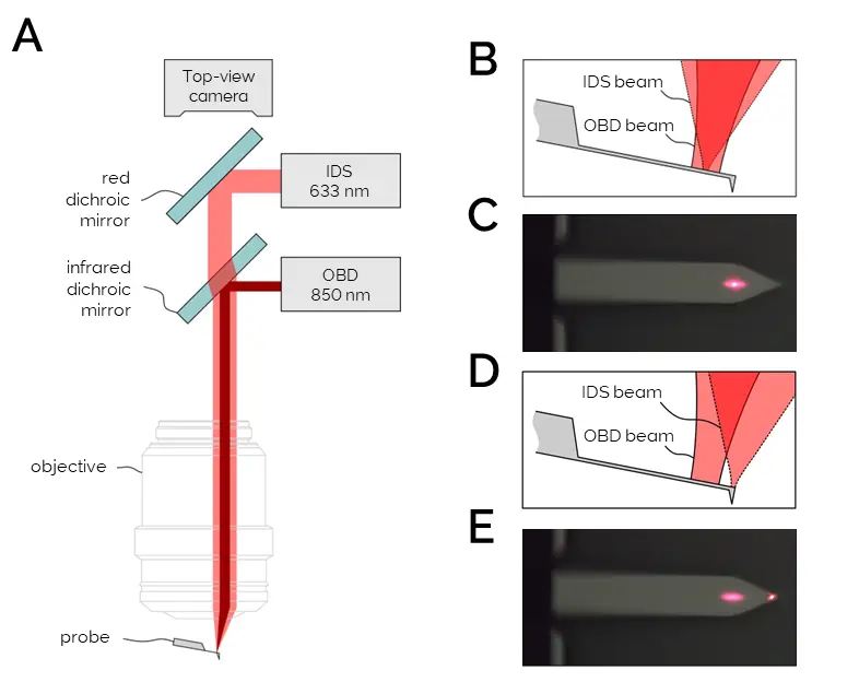
In response to these shortcomings of OBD for PFM measurements, Oxford Instruments Asylum Research developed the Cypher Interferometric Displacement Sensor (IDS) AFM.1 This AFM incorporates a laser Doppler vibrometer (LDV) that can interferometrically measure the cantilever deflection concurrently with the standard OBD technique (Figure 3). Interferometric detection offers several benefits over OBD:
- It directly measures cantilever displacement (vs. OBD, which is proportional to angle).
- The measurement is inherently calibrated by the wavelength of the laser (vs. OBD, which requires calibration each time it is adjusted).
- Its cantilever deflection noise floor is 2 - 3× lower than typical OBD performance (typ. <100 fm/√Hz).
Most critically for PFM measurements, however, is that the LDV laser spot can be positioned precisely over the probe tip (Figure 4D-E). In that position, the LDV measurement is sensitive to only actual tip displacement and is not influenced by the mode shapes of the cantilever resonances. As we will see next, this allows PFM measurements to be made while eliminating the troublesome electrostatic artifact.
PFM measurements of Periodically Poled Lithium Niobate (PPLN)
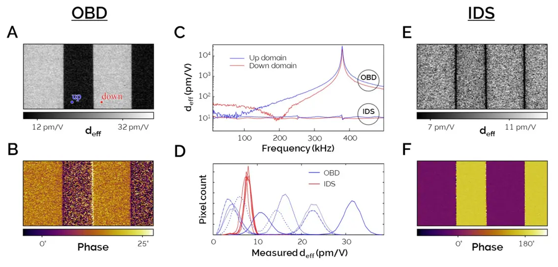
A common test sample for PFM is periodically poled Lithium Niobate (PPLN), which is expected to exhibit frequency-independent response, equal amplitude response independent of polarization direction, and a 180° phase shift across oppositely poled domains. As shown in Figure 4A-C, none of these expected characteristics match what is observed in actual PFM measurements made with conventional OBD cantilever deflection measurement. Additionally, repeated measurements of the effective coupling coefficient yield vastly different results (Figure 4D). These contradictions clearly indicate a problem with the measurement, but only recently could it be clearly attributed to the electrostatic artifact.
In summary, these electrostatic artifacts related to optical beam detection can lead to great uncertainty in the interpretation of PFM results. They can lead to false signatures of ferroelectricity in the form of hysteretic switching spectroscopy loops, making it difficult to use those measurements to identify ferroelectric materials. The artifacts also result in very inconsistent measurements of piezoelectric response, d33, making it difficult to quantitatively compare different piezoelectric or ferroelectric materials. Considering that both are very common objectives of PFM measurements, eliminating these artifacts is crucial.
The ability of an AFM with interferometric detection (such as the Asylum Research Cypher IDS) to directly measure tip displacement without the influence of electrostatic forces enables PFM measurements that match predicted PPLN behaviour (Figure 4E-F) and are highly repeatable (Figure 4D).
Conclusion
The Cypher IDS, resulting from a fruitful cooperation between Oxford Instruments Asylum Research and Polytec, has become the gold standard for electromechanical characterization of piezo and ferroelectrics. Its ability to measure the electromechanical response without the influence of electrostatic artifacts enables both the unambiguous measurement of polarization switching hysteresis loops in ferroelectrics and, for the first time, highly repeatable measurement of the electromechanical coupling coefficient in both piezoelectrics and ferroelectrics.
References
1. A. Labuda and R. Proksch, Appl. Phys. Lett. 106, 253103 (2015).
This article is an adaptation of the application note by Oxford Instruments Asylum Research Inc.: Cypher IDS AFM Enables More Quantitative Piezoresponse Force Microscopy