The technology of printed electronics has moved beyond the pioneering stage, and the first industrial applications are already underway. Potential applications are diverse, but turnkey system solutions that make it easier for industrial customers to get started have so far been lacking.
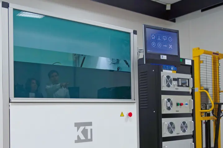
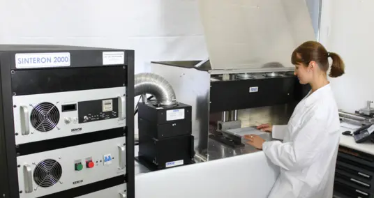
Kelenn Technology, a French printer manufacturer and imaging solutions provider, has launched an inkjet printer for printed electronics. Using metallic nanoparticle inks, it can print electronic circuits on A4-sized flexible substrates such as paper, film, or textiles—automated and at volumes of up to 10,000 sheets per day.
Didier Rousseau, CEO and founder of Kelenn Technology, spoke with Polytec about the development of the KSCAN PE.

What does your company do, Mr. Rousseau?
Kelenn was founded in 2005. At our headquarters in Paris, we employ 23 people, and we currently have two branches in the USA and India. We manufacture imaging systems, printers for industrial applications, and the corresponding software.
Our inkjet printers are mainly delivered to customers who use them in postal applications for addressing, franking, transactions, direct mailings, but also in document security, packaging, film applications, and printed electronics. Our industrial imaging systems perform tasks such as identification, object tracking, inspection, measurement, and sorting in large-scale, high-speed production processes.
"Kelenn aims to reduce customer production costs while adding value through 100% quality control."
What was the focus in developing the new KSCAN PE?
In the printed electronics market, there are various technologies to print conductive inks on different substrates. One of these is inkjet technology, whose clear advantage lies in the high precision of the printing results. However, the process comes with many challenges, such as repeatability and durability of the results. We wanted to create an all-in-one printing system for industrial production environments that combines inkjet printing of conductive inks with the sintering process. This is necessary to produce long-lasting, conductive connections. The system should handle different substrates in single sheets up to A4 size at high throughput.
And that’s where Polytec came in for the sintering?
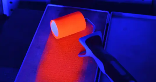
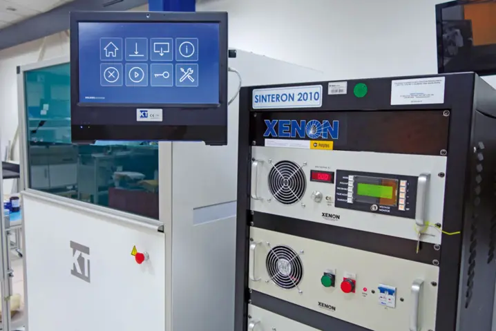
"Polytec was the ideal development partner for the project because the company brought extensive know-how in the photonic sintering process and has represented the American UV flash system manufacturer, Xenon Corporation, in Europe for years."
Were there any alternatives to the Xenon sintering systems?
Not really. Xenon was essentially without alternative, as we aimed for an industrial-ready solution capable of handling high cycle rates and large production volumes. Other technologies, such as thermal sintering in ovens, were not suitable because the sintering process there takes significantly longer. Additionally, it involves high heat input into the substrate, which excludes heat-sensitive materials like films.
With photonic sintering, there are often concerns about achieving uniform sintering results over larger areas—so-called “stitching.” And an A4-sized area isn’t trivial—how did you handle that?
We sinter the area using a U-shaped flash lamp and multiple pulses. We have no issues with stitching, i.e., overlaps or underexposure at the edges of the effective area.
How was Polytec’s support during the project?
Polytec provided strong support throughout the development. On one hand, through their already mentioned deep know-how of the sintering process. On the other hand, we were able to test Xenon systems over several months to prove feasibility and ensure integration. During this time, Polytec frequently offered valuable feedback and on-site consulting, helping us align the sintering process with the other production steps and make it suitable for industrial use.
Could the system development be completed as planned?
Not entirely (laughs). Printing metallic nanoparticle inks in combination with the sintering process is a very complex procedure that took us over a year of development time. We encountered phenomena that were completely new to us and had to change the ink composition countless times, which in turn directly affected the printing and sintering processes. It was a very time-consuming, tough job.
What is the main advantage of the KSCAN PE?
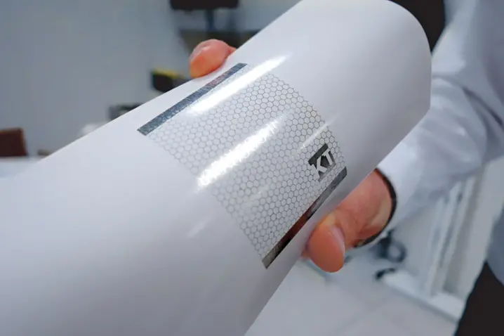
Actually, one could even speak of 5 advantages: Firstly, thanks to the photonic sintering process, we achieve an outstanding production speed of 10,000 sheets per day. Then we can print on various flexible and heat-sensitive substrates such as paper, films, textiles, etc. The third advantage is that, in a certain way, we can also 3D print, i.e., create raised structures on the substrate. Fourthly, the precision of the inkjet technology allows for minimum layer thicknesses of 200 nanometers with consistent conductivity of 100 milliohms per square centimeter. This makes the technique significantly more efficient than, for example, screen printing. And this directly results in lower costs for the silver-containing inks.
Last but not least, it must of course be mentioned that Kelenn is the first company to deliver a turnkey all-in-one system.
And for which markets is the system interesting?
There are many potential applications, given the numerous printable substrates. A main current application is the printing of RFID antennas for object tracking. But OLEDs, batteries, or organic photovoltaic circuits can also be printed. We currently see the main market in the medical and healthcare sector, where RFIDs find diverse applications thanks to their small size and flexibility.
And what conclusion would you draw from today’s perspective?
Without Polytec, we would not have been able to realize this innovative solution. We plan to continue on this path together and further develop the system to explore and implement many more applications.